Aug 17

It's time to think about the SC-3000X enclosure...


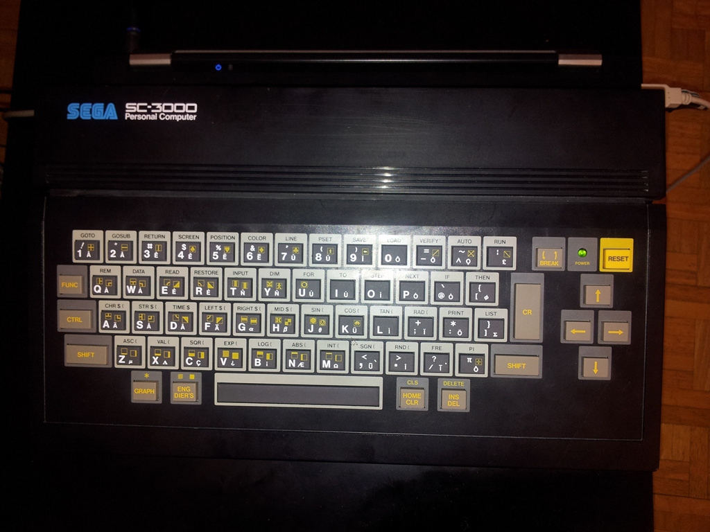
The original SC-3000? Uh?


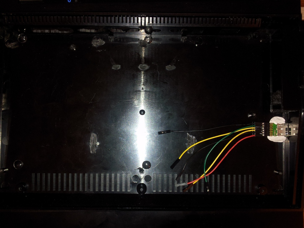
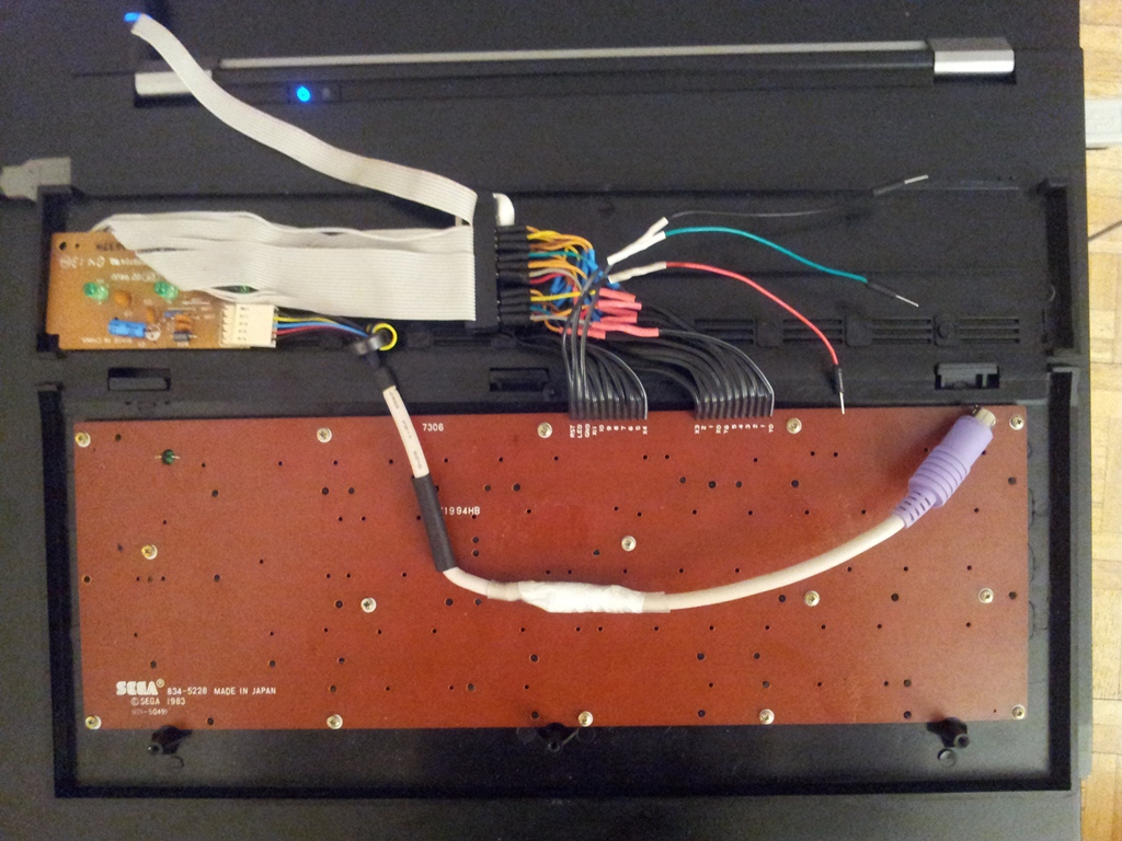
Inside view. Original mobo removed, flatten space, my Dremel does the job! Trioflex microSD card adapter present on right, fixed on plastic with UHU Patafix (needed some final solution).


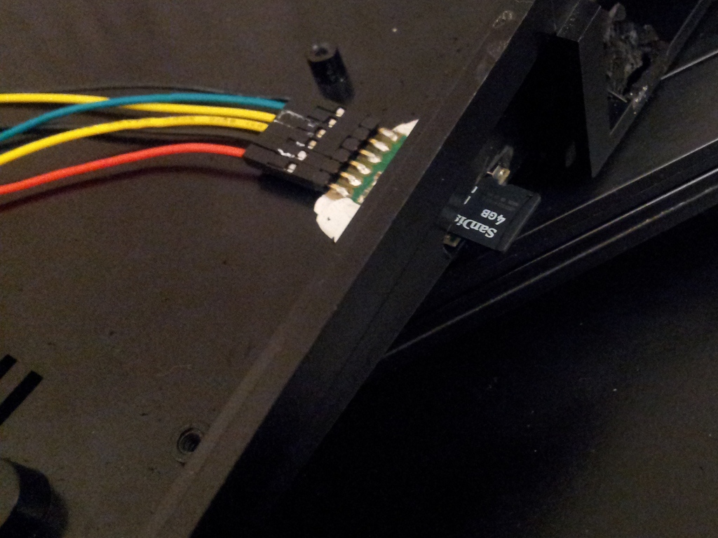
Detail of microSD adapter with microSD inside (4GB).


Original keyboard connected (through floppy cable) to PS/2 controller card got from an old PC keyboard. Total remap of keys was done!


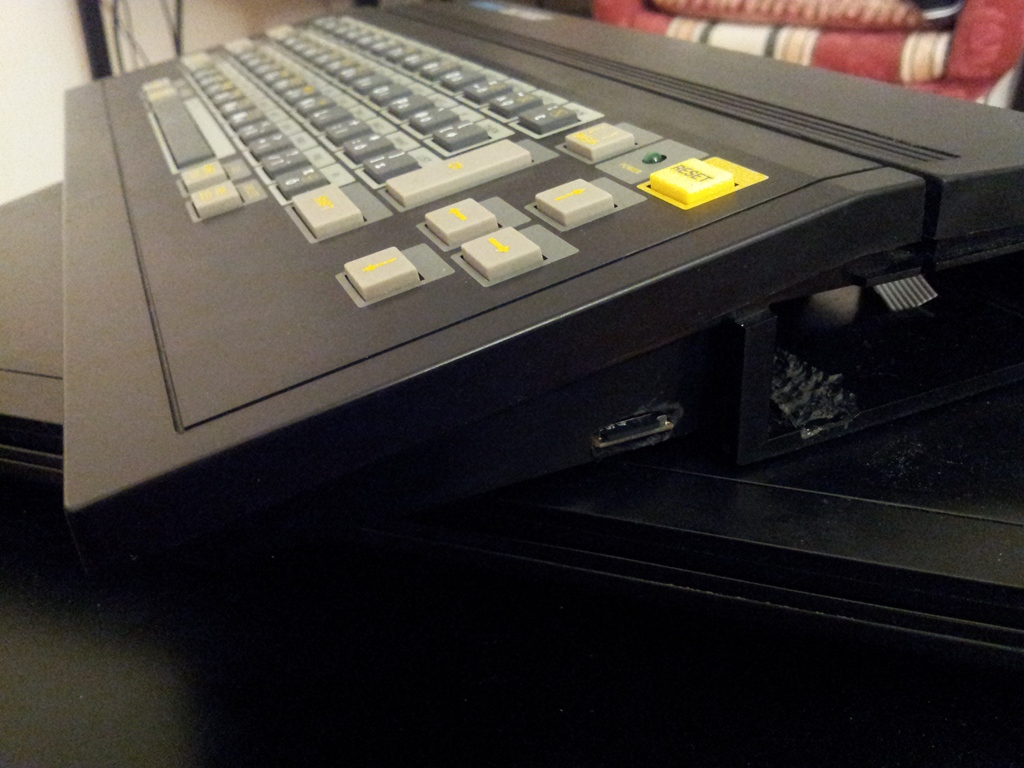
Right view of modified enclosure.


Jun 13

Yeah!!!

Finally an almost stable implementation of FAT32 filesystem in SD-5000 integrated sdcard interface.

Enjoy...

Sep 19

This is my first beta version of the TMS9928 VDP Mode 2 implementation.
Sprites are not finished yet, so not included.
System main clock is 21,42857 Mhz (50 * 3 / 7) but VGA is running at 25Mhz.
A line-based buffering allows the clock synchronization.

SDcard loader are faster now using MasterClock / 2,
but it's track based and no FAT is supported yet.
The video shows the system startup 2 times in order to underline the new SD loader speed.

Enjoy...


Sep 17

Finally!!!

This time your eyes are pleasured by my first attempt to recreate SEGA SC-3000 home computer (1983).

Through this video you can see my IPL rom loading original SEGA BasicLevel 3A from SDcard.

After loading 32KB of data into RAM, the IPL rom deactivate itself rebooting into loaded data.

Enjoy...


Sep 12

SDCARD! Finally an almost correct initialization.

On first row onto the screen we can see the initialization commands prefixed by ">" character.

We can see CMD0, CMD59, CMD8, ACMD41, CMD16 and finally CMD17 (READ_SECTOR).

The data is written onto sdcard starting from sector 0 using a sector-editor, in order to avoid (by now) FAT routines implementation.

The screen shows on second row the data from 0x0100 to 0x01FF (256 bytes) of SEGA BASIC Cart.


Sep 05

Textmode! 40x24, 240x192 pixels + borders. 6x8 chars.

The SC-3000 has CPU access limitations during display time.

The SC-3000X can access to VRAM during display area 1 time every char row.

VRAM accesses are done using ports $BE/$BF.


Jul 18

This time my Altera DE1 hosts 5 complex components:

1) Clock engine that uses an onboard PLL. It supply the MasterClock at 21,428Mhz, the SDRAM/Controller clock at  85,712Mhz and VGA clock at 25Mhz.

2) Z80 cpu core (T80SE core) running at a fraction of original 3,58Mhz and uses the Altera DE1 onboard SDRAM as RAM/ROM source.
The assembler program starts copying itself into RAM (SDRAM) at $E000 then jump to that address.
Then copy the characters bitmap data into RAM used by VDP core at $A800 (VRAM).
After this it change row by row the name table at address $A000 that VDP uses as tile number source. 

3) A simple tile-based VDP controller that uses the same SDRAM as nametable (tile numbers) and tiletable (tile bitmap data).
The VDP core uses the MASTERCLOCK as clock source and the image resolution is 288x240.
The pixel-clock is 5,357Mhz (MASTERCLOCK/4).
It prefetches 8 pixels of data in order to avoid the trace flickering.

4) Double buffered 25Mhz VGA scaler that transforms the VDP created data and adds lateral black border.
The engine manages VGA screen at 640x480 pixel doubling also the pixel size.

5) Dual port SDRAM controller that manage onboard SDRAM chip (Zentel A3V64S40ETP).
The controller it used as RAM access arbiter between CPU and VDP.
It's clocked at 85,712Mhz (MASTERCLOCK x 4). Only auto-precharged/one-burst-length access are used (READA/WRITA).
Any access is served in 8 SDRAM clocks producing 10Mhz bandwith that are shared between CPU and VDP engines.


Tags: | | | | |
Jul 04

My low-level UART / RS232 routines are almost ready.

It uses 115200/8N2 (11 bits for each byte) as parameters allowing a data trasfer rate of ~10KBytes/sec.


Data trasfer into the video was done using a PC with Windows 7 and a USB2Serial cable from Hama with Prolific chip.


Altera DE1 onboard UART works well!


Tags:
Apr 11

Finally I decided to start a new project...

Project? What project? Click here to learn more.

Tags: | | |
Apr 11

Hello there, today I will introduce you my brand new Altera DE1 FPGA Development Board.

Yeah! This board substitutes my Xilinx Spartan 3AN for a while, due to difficults in RAM usage (DDR2) of this board and lacking for other features (decent audio DAC, SRAM, SD slot,...).

Altera DE1 has many good and interesting features like:

  • Cyclone II EP2C20F484C7 (18,752 Logic Elements, 52x M4K 4kbits ram blocks, 234kbits embedded memory, 26x 18-bit x 18-bit multipliers, 4 PLL, 315 I/O pins)
  • EPCS4 4-Mbit serial configuration device programmable to store the FPGA configuration autoloaded on start
  • 512KByte SRAM (256x16bit asynchronous, very very useful and simple to program)
  • 8MB DRAM (synchronous DRAM but not hard-to-use as DDR2 one)
  • 4MB Flash RAM
  • 1x 50Mhz Clock
  • 1x 27Mhz Clock
  • 1x External SMA clock input
  • 12bit VGA DAC (4096 colors on screen is enough for many things)
  • 24bit Audio CODEC with lin-out, line-in, mic-in connectors (wow! how many beautiful things can we do with a similar audio DAC!!!)
  • Onboard SD card slot (yeah! useful to access external data like... ROMS....)
  • PS/2 keyboard connector
  • 10 red LEDs, 8 green LEDs, 10 switches
  • 4x debounced pushbuttons
  • 4x 7-segments display
  • 2x IDE expansion headers to accessing external devices/resources
  • 1x RS-232 (useful to monitor/debug application from PC)

Tags: | | |